#current
Documents
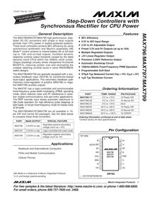
General Description The MAX796 MAX797 MAX799 high performance step down DC DC converters with single or dual outputs provide main CPU power in battery powered systems These buck controllers achieve efficiency by using synchronous rectification and Maxim's proprietary Idle Mode™ control scheme to extend battery life at full load up to 10A and no load outputs Excellent dynamic response corrects output transients caused by the latest dynamic clock CPUs within five 300kHz clock cycles Unique bootstrap circuitry drives inexpensive N channel MOSFETs reducing system cost and eliminating the crowbar switching currents found in some PMOS NMOS switch designs The MAX796 MAX799 are specially equipped with a sec ondary feedback input SECFB for transformer based dual output applications This secondary feedback path improves cross regulation of positive MAX796 or nega tive MAX799 auxiliary outputs The MAX797 has a logic controlled and synchronizable fixed frequency pulse width modulating PWM operating mode which reduces noise and RF interference in sensi tive mobile communications and pen entry applications The SKIP override input allows automatic switchover to idle mode operation for high efficiency pulse skipping at light loads or forces fixed frequency mode for lowest noise at all loads The MAX796 MAX797 MAX799 are all available in pin DIP and narrow SO packages See the table below to compare these three converters

Documents
Rapports de stage
General Description The MAX796 MAX797 MAX799 high performance step down DC DC converters with single or dual outputs provide main CPU power in battery powered systems These buck controllers achieve efficiency by using synchronous rectification and Maxim's proprietary Idle Mode™ control scheme to extend battery life at full load up to 10A and no load outputs Excellent dynamic response corrects output transients caused by the latest dynamic clock CPUs within five 300kHz clock cycles Unique bootstrap circuitry drives inexpensive N channel MOSFETs reducing system cost and eliminating the crowbar switching currents found in some PMOS NMOS switch designs The MAX796 MAX799 are specially equipped with a sec ondary feedback input SECFB for transformer based dual output applications This secondary feedback path improves cross regulation of positive MAX796 or nega tive MAX799 auxiliary outputs The MAX797 has a logic controlled and synchronizable fixed frequency pulse width modulating PWM operating mode which reduces noise and RF interference in sensi tive mobile communications and pen entry applications The SKIP override input allows automatic switchover to idle mode operation for high efficiency pulse skipping at light loads or forces fixed frequency mode for lowest noise at all loads The MAX796 MAX797 MAX799 are all available in pin DIP and narrow SO packages See the table below to compare these three converters
32 pages
English
Documents
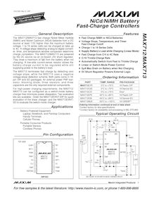
General Description The MAX712 MAX713 fast charge Nickel Metal Hydride NiMH and Nickel Cadmium NiCd batteries from a DC source at least 5V higher than the maximum battery voltage to series cells can be charged at rates up to 4C A voltage slope detecting analog to digital convert er timer and temperature window comparator determine charge completion The MAX712 MAX713 are powered by the DC source via an on board +5V shunt regulator They draw a maximum of 5m A from the battery when not charging A low side current sense resistor allows the battery charge current to be regulated while still supplying power to the battery's load The MAX712 terminates fast charge by detecting zero voltage slope while the MAX713 uses a negative voltage slope detection scheme Both parts come in pin DIP and SO packages An external power PNP tran sistor blocking diode three resistors and three capacitors are the only required external components For high power charging requirements the MAX712 MAX713 can be configured as a switch mode battery charger that minimizes power dissipation Two evaluation kits are available: Order the MAX712EVKIT DIP for quick evaluation of the linear charger and the MAX713EVKIT SO to evaluate the switch mode charger
Max Drain

Documents
Annales d’examens et concours
General Description The MAX712 MAX713 fast charge Nickel Metal Hydride NiMH and Nickel Cadmium NiCd batteries from a DC source at least 5V higher than the maximum battery voltage to series cells can be charged at rates up to 4C A voltage slope detecting analog to digital convert er timer and temperature window comparator determine charge completion The MAX712 MAX713 are powered by the DC source via an on board +5V shunt regulator They draw a maximum of 5m A from the battery when not charging A low side current sense resistor allows the battery charge current to be regulated while still supplying power to the battery's load The MAX712 terminates fast charge by detecting zero voltage slope while the MAX713 uses a negative voltage slope detection scheme Both parts come in pin DIP and SO packages An external power PNP tran sistor blocking diode three resistors and three capacitors are the only required external components For high power charging requirements the MAX712 MAX713 can be configured as a switch mode battery charger that minimizes power dissipation Two evaluation kits are available: Order the MAX712EVKIT DIP for quick evaluation of the linear charger and the MAX713EVKIT SO to evaluate the switch mode charger
Max Drain
18 pages
English
Documents
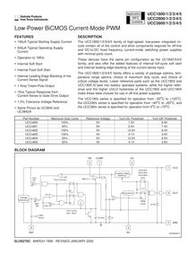
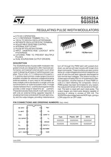
REGULATING PULSE WIDTH MODULATORS TO V OPERATION V REFERENCE TRIMMED TO Hz TO KHz OSCILLATOR RANGE SEPARATE OSCILLATORSYNC TERMINAL ADJUSTABLE DEADTIME CONTROL INTERNAL SOFT START PULSE BY PULSESHUTDOWN INPUT UNDERVOLTAGE LOCKOUT WITH
Stmicroelectronics

Documents
Rapports de stage
REGULATING PULSE WIDTH MODULATORS TO V OPERATION V REFERENCE TRIMMED TO Hz TO KHz OSCILLATOR RANGE SEPARATE OSCILLATORSYNC TERMINAL ADJUSTABLE DEADTIME CONTROL INTERNAL SOFT START PULSE BY PULSESHUTDOWN INPUT UNDERVOLTAGE LOCKOUT WITH
Stmicroelectronics
12 pages
English
Documents
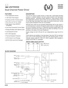
DESCRIPTION The UC1707 family of power drivers is made with a high speed Schottky process to interface between low level control functions and high power switching devices particularly power MOSFETs These devices contain two independent channels each of which can be activated by either a high or low input logic level signal Each output can source or sink up to 5A as long as power dissipation limits are not exceeded Although each output can be activated independently with its own inputs it can be forced low in common through the action either of a digital high sig nal at the Shutdown terminal or a differential low level analog signal The Shutdown command from either source can either be latching or not de pending on the status of the Latch Disable pin Supply voltage for both VIN and VC can independently range from 5V to 40V These devices are available in two watt plastic bat wing DIP for operation over a 0°C to 70°C temperature range and with reduced power in a her metically sealed cerdip for –55°C to +125°C operation Also available in surface mount DW Q L packages
Line Package

Documents
Rapports de stage
DESCRIPTION The UC1707 family of power drivers is made with a high speed Schottky process to interface between low level control functions and high power switching devices particularly power MOSFETs These devices contain two independent channels each of which can be activated by either a high or low input logic level signal Each output can source or sink up to 5A as long as power dissipation limits are not exceeded Although each output can be activated independently with its own inputs it can be forced low in common through the action either of a digital high sig nal at the Shutdown terminal or a differential low level analog signal The Shutdown command from either source can either be latching or not de pending on the status of the Latch Disable pin Supply voltage for both VIN and VC can independently range from 5V to 40V These devices are available in two watt plastic bat wing DIP for operation over a 0°C to 70°C temperature range and with reduced power in a her metically sealed cerdip for –55°C to +125°C operation Also available in surface mount DW Q L packages
Line Package
8 pages
English
Documents
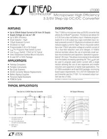
N Up to 220mA Output Current at 5V from 2V Supply n Supply Voltage as Low as 8V n Up to Efficiency n Small Inductor H n A Quiescent Current n Shutdown to A n Programmable 3V or 5V Output n ILIM Pin Programs Peak Switch Current n Low VCESAT Switch: 170mV at 1A Typical n Uses Inexpensive Surface Mount Inductors n Lead DIP or SOIC Package

Documents
Cours
N Up to 220mA Output Current at 5V from 2V Supply n Supply Voltage as Low as 8V n Up to Efficiency n Small Inductor H n A Quiescent Current n Shutdown to A n Programmable 3V or 5V Output n ILIM Pin Programs Peak Switch Current n Low VCESAT Switch: 170mV at 1A Typical n Uses Inexpensive Surface Mount Inductors n Lead DIP or SOIC Package
8 pages
English
Documents
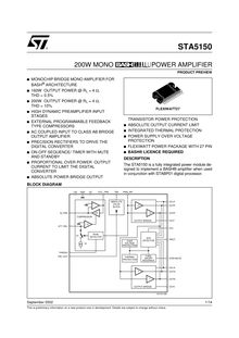
September This is preliminary information on a new product now in development Details are subject to change without notice
Stmicroelectronics
Documents
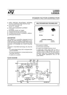
VERY PRECISE ADJUSTABLE INTERNAL OUTPUT OVERVOLTAGE PROTECTION HYSTERETIC START UP ISTART UP 5mA VERY LOW QUIESCENT CURRENT 5mA INTERNAL START UP TIMER TRANSITION MODE OPERATING TOTEM POLE OUTPUT CURRENT: ±400mA DIP8 SO8 PACKAGES
Stmicroelectronics

Documents
Corrigés de devoir
VERY PRECISE ADJUSTABLE INTERNAL OUTPUT OVERVOLTAGE PROTECTION HYSTERETIC START UP ISTART UP 5mA VERY LOW QUIESCENT CURRENT 5mA INTERNAL START UP TIMER TRANSITION MODE OPERATING TOTEM POLE OUTPUT CURRENT: ±400mA DIP8 SO8 PACKAGES
Stmicroelectronics
11 pages
English
Documents
Diseño y consideraciones de un lazo de compensación para el convertidor tipo boost (elevador) cd-cd controlado en modo de voltaje (Design and considerations of a compensation lace for the converter- booster dc-dc controlled in voltage mode)
David
Collection
{{collectionTitle}}
Collection
{{collectionTitle}}
Collection
{{collectionTitle}}
{{productCategoryLabel}}
{{productTitle}}
{{productAuthors}}
{{productCategoryLabel}}
{{productThemeLabel}}
{{productTitle}}
{{productAuthors}}
{{productPages}}
{{productLanguageIsoCode}}

